Semiconductors combine divinity and science. Not long ago we created a blog based on the steps of manufacturing semiconductors. We dutifully and scientifically cataloged the steps to making a semiconductor.
With this ER Precision Optics blog, we strive to penetrate the secrets behind those steps. Likewise, we acknowledge Moore’s Law as integral to the history of semiconductors.
The Backstory: Moore’s Law
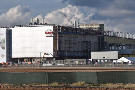
This is the TSMC Plant in Phoenix, AZ. And Like the Largest Plant in the World, Taiwan, It Appears Simple on the Outside. However, It Hides Divine Complexity on the Inside.
Although this is technically Part II of our most recent blog, it also stands alone in its own right. We suggest you might enjoy reading the story of Moore’s Law, as written in our most recent blog before looking beyond the factual and into the divine in this story.
The Manufacture of Chips: From Humorous to Mystical
So, why is creating these essential chips so difficult and so expensive? These are the questions people continue to ask when the conversation turns to Chips. There is both a simple answer and a complicated one.
As we stated, “The simple version is that making chips is incredibly difficult—and getting tougher. It’s also immensely expensive.” And we cited Bloomberg’s inside industry joke. He said, “It’s not rocket science—it’s much more difficult.”
The Divine World of Semi-conductor Creation
However, in a recent article from Wired, the journalist, Virginia Hefferman infused metaphysical beauty in her ruminations on chip manufacturing. In fact, she entitled her article, “I Saw the Face of God in a Semiconductor Factory.”
We were intrigued by her almost mystical observations. So, we thought we would share some of them interlaced with the known facts about chip manufacturing factories.
Perhaps her thoughts will help us illuminate the beauty and curiosity of Chip workers and chip science, and the US commitment to new factories of our own. We call such factories “fabs.” Of course, soon the US will have its own gigantic one in Arizona, but that’s another story.
Semiconductor Factories Meld Divinity with Science
Hefferman visited none other than the largest chip factory in the world, TSMC in Taiwan. So, we preface this article by saying it is no wonder she was impressed. TSMC is bigger than Exon and bigger than Meta. In short, experts estimate TSMC (Taiwan Semiconductor Manufacturing Corporation creates about 92% of the world’s most complex chips.
According to Hefferman, the corporation also makes most of the world’s most complicated semiconductors inside “nuclear weapons, planes, submarines, and hypersonic missiles…” And she added that such semiconductors are the fabric “on which the international balance of hard power is predicated.”
Chip Basics: What is a Semiconductor?
One Slide of Silicone Can Yield Thousands of Semiconductors. And This is Why TSMC Encourages Scientists to Think at the Atomic Level. Only Then Can Moore’s Law Reign Supreme.
The end goal is to transform wafers of silicon into a network of billions of tiny transistors. These transistors create the basis of the circuitry that will be the heartbeat of your cellphone, car, or satellite.
To put it briefly, most chips are miniature groups of circuits. They “run the software and manipulate data…” Thus, they control the functions of various electronic devices.
The Nitty Gritty Basics of Creating Chips: Six Amazing Basic Steps to Creating Semiconductors
To make any chip, numerous processes must all play a meticulous role. In our previous article, we briefly investigated 6 essential steps in creating a semiconductor. The steps are listed as deposition, photoresist, lithography, etching, ionization, and packaging.
You might want to read that blog as a scientific, factual review of all 6 steps. Read and review it, because the purpose of today’s blog is to explore beyond the mere facts of semiconductors. We want to go deeper into the mysterious feelings provoked by seeing or even imagining the process of creating semiconductors.
Why We Care Deeply About Mighty but Miniscule Semiconductors
You probably know that ingots of silicon are the beginning of a semiconductor sandwich.
Thus, since ER Precision Optics grows silicon crystals, we are very involved with the life of semiconductors. And yes, we think about it a lot!
TSMC: Showing How Semiconductors Meld Divinity and Science.
On the Edge of Invisible – In R&D, They Envision an Atom-Sized Semiconductor. And That is Almost Divinity Melded in Science.
At TSMC as well as many other semiconductor factories, the processing begins with world trade.
1. First, “Companies like Sumco, in Japan, process polycrystalline silicon sand.”
2. Preliminary to this process, world-class companies quarry the silicon sand “in places like Brazil, France, and the Appalachian Mountains…” For TSMC. Global trade is essential to creating semiconductors and part of the magic of melding divinity with science.
3. At the factory, Hefferman states, single-crystal silicon ingots must be sliced. She elaborates, “With diamond wire saws, Sumco’s machines slice shimmering wafers…” She adds that TSMC polishes them “so smooth they feel like nothing under a fingertip, are the flattest objects in the world.”
The Next Step Away from Science to Sublime
Hefferman declares that some wafers are up to a foot in diameter. Into TSMC’s automated machines, they go for photolithography and identity. With photolithography, the machines “etch billions of transistors onto each chip-sized portion…”
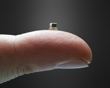
To give you an idea of the scale of this undertaking, “the biggest wafers yield hundreds of chips.” Hence, “Each transistor is about 1,000 times smaller than is visible to the naked eye.” That puts the micro in the microprocessor.
The Factory Tour Melds Divinity and Science in the Lithography Step of Semiconductor Creation
In the space of a blog, we can not discuss every step from silicon to semiconductor. However, we have already referred you to our 6-step blog.
However, we will elaborate on the Lithography Step, which Hefferman found especially inspiring.
She highlights her thoughts with poetic descriptions. We’ll give you the main points, but to see the poetry behind the marriage of divinity and science, you might have to read her entire 38-page article, based on her tour of TSMC’s fab #12 factory.
Semiconductors Meld Divinity and Science: Transubstantiation
The magic begins, as we stated above, with thin slices of the purest silicon crystal.
- From there, “A projector, its lens covered by a crystal plate inscribed with distinctive patterns…” arches over the wafer.” That crystal plate could be the blueprint for your cell phone or a Cruise missile.
- The machines then beam extreme ultraviolet light through the plate and onto the wafer.
- This procedure prints “A design on it before it’s bathed in chemicals to etch along the pattern.”
Repeat and Repeat, Like a Mystical Spell
As if printing on money or fine porcelain, “This happens again and again until dozens of latticed layers are printed on the silicon.”
The Final Amazing Step to Meld Divinity and Science
At last, technicians cut the chips out of the wafer. “Each chip, with billions of transistors stacked on it, amounts to an atomic multidimensional chessboard with billions of squares.” Each chip has an infinite number ons and offs.
The Lithography Step: Divinity Tolerates No Errors
Naturally, as we have stated in previous blogs, there is no tolerance for error. In each of the above steps, the patterning must be perfect. TSMC tolerates no particle interference, refraction, or chemical defects. LINK:
Of course, there are many sub-steps we do not describe in this article. But in this blog, remember, we are concerned with the vision. What does this vision look like, from the floor of a TSMC factory where semiconductors meld divinity with science?
Virginia Hefferman’s Vision
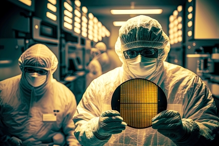
Swathed in a clean suit and slippers, mask, and goggles, Virginia Hefferman described the vision which some observers would only see as assembly line tedium. But as she saw the workers and technicians bent on their tasks, she described wondering at the atomic level.
As she observed, she spoke. “I walk very slowly. The white humming machines are featureless…” She adds,
“And thick hermetic glass stands between me and the fathomless nano-processes that I couldn’t have perceived with my crude pupils anyway.”
Explaining the Vision of Working Nanotech Technology

The Moment of Divine Inspiration: Micro-laser Processing of Semiconductor Nano Components Melding Creative Divinity With Science.
“It dawns on me at once that the machines resemble incubators in a neonatal intensive care unit. Inside them, something very fragile flickers between existence and whatever comes before existence.” And it all works to the heartbeat of Moore’s Law. Here Moore’s Law still lives: “Half the size, double the profit.”
Here, the creative processes appeared lifesaving. She saw the wafers, chips, and chemical processes as a sort of neonatal intensive care unit. She wrote, “Tiny souls that must be protected from less than a nano of gas are surely immunocompromised. I picture the transistors as trembling bodies with translucent skin and fast, shallow breaths.”
What’s more, she saw tenderness. The semiconductors resembled embryos. “They are utterly dependent on adults who cherish them for their extraordinary smallness and cosmic potential.”
She concluded, “What’s present here is preciousness. To see the fabs is to feel a full-body urge to keep the tiny marvelous creations—newborns—and then humanity as a whole—alive.”
And she ruminates throughout the article that perhaps this alliance between divinity and science will keep us—and democracy—alive.