Creating semiconductors seems to be an easy answer to current shortages plaguing the US industry. However, this may not be as easy as it seems.
In Part I of our previous semiconductor blog topic, we investigated this shortage. In fact, you might want to read that article before you check out this one.
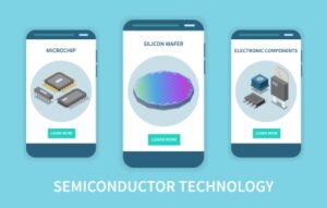
Creating Semiconductors

The Auto Industry is Sounding the Alarm Over Lost Dollars Due to Semiconductor Shortages.
As we revealed in our previous article, our nation’s automakers are preparing to lose billions of dollars due to the shortages. Semiconductor Chips are critical to the auto industry. They use them to make a huge repertoire of elements that power your car.
1. For example, you need them to create modern steering and braking systems.
2. Additionally, semiconductors are used in “intelligent functions such as blind-spot detection, adaptive cruise control, and lane change assist.”
3. Last but not least, especially if you are a parent with a minivan. They are essential in vehicular infotainment systems. This is not surprising since semiconductors are the brains behind almost all the electronic gadgets that power our 21st-century lives.
As stated previously, “According to CNBC, automakers are ‘scrambling to get supplies of the chips…” And they added the big reason. These tiny elements have “extremely long lead times due to their complexity.”
Semi-Conductor Chips: Rocket Science or Mission Semi-Impossible
Creating Semiconductors Involves 3 Im,portant Technologies.
So, why is creating these essential chips so difficult? What is the secret
recipe? These are the questions we hope to answer with this ER Optics blog.
There is both a simple answer and a complicated one. The simple version is that making chips is incredibly difficult—and getting tougher. It’s also immensely expensive. As Bloomberg recently stated, “It’s not rocket science—it’s much more difficult,” is one of the industry’s inside jokes.
The Stunning Complexity of Creating Semiconductors
As we have explained before, it takes many years and dollars to create the fabrication facilities for creating semiconductors. Therefore creating a chip requires a major effort.
- Time is money and making a chip takes more than 3 months.
- Creating microchips also requires clean rooms that are dust-free. And we do mean clean—even cleaner than surgical rooms.
- Likewise making chips means “multi-million-dollar machines, molten tin, and lasers.”
Chip Basics: What is a Semiconductor?
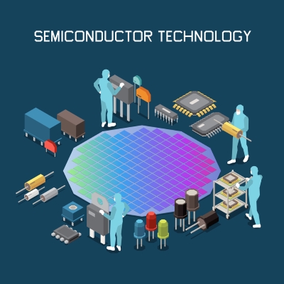
The end goal is to transform wafers of silicon into a network of billions of tiny transistors. These transistors create the basis of the circuitry that will be the heartbeat of your cellphone, car, or satellite.
To put it briefly, most chips are miniature groups of circuits. They “run the software and manipulate data…” Thus, they control the functions of various electronic devices.
The Nitty Gritty Basics of Creating Chips: Six Amazing Basic Steps to Creating Semiconductors
To make any chip, numerous processes must all play a meticulous role. For our purposes, let’s investigate only the basic 6 essential steps in creating a semiconductor. They are listed as deposition, photoresist, lithography, etch, ionization and packaging.
1. First Comes the Deposition

Meticulous Inspection of Semiconductors After Every Step is a Vital Part of the Process.
As you know from our previous article, concerning ingots of silicon, this is where the process starts. First, imagine a long gray metallic meatloaf called an ingot of silicon—and not just any silicon. To qualify for this procedure, the silicon must be 99.9% pure silicon. The manufacturer thinly slices a wafer of silicon from an ingot of 99.9% pure silicon.
Then they apply micro-thin films of various conducting, isolating, or semiconducting materials. The types of film applied to depend on the type of chip involved. Therefore, it is named the Deposition step in the procedure of creating a semi-conductor. (That gives casual readers a whole new meaning to chip and dip, doesn’t it?)
2. Second Concern in Creating a Semiconductor: Photoresist Coating—More Dip for Our Chip
Next, the wafer must be completely covered with a light-sensitive coating. called ‘photoresist’, or ‘resist’ for short. It is valuable to know that there are two types of resistance: positive and negative. Let’s examine this more closely.
- Two outstanding differences rule the world of “Resist.” One is the chemical structure of the material. And the other is the way the resist reacts when exposed to light.
- When the coating of choice is positive resist, “the areas exposed to ultraviolet light change their structure and are made more soluble – ready for etching and deposition.”
- When the manufacturer chooses negative resist, then areas hit by light polymerize. This simply means they “become stronger and more difficult to dissolve.”
So, What is the Most Common Resist?
Positive resist is most used in creating semiconductors. The reason is that “its higher resolution capability makes it the better choice for the lithography stage.”
You might like to know that “Several companies around the world produce resist for semiconductor manufacturing…” They have some familiar names such as “Fujifilm Electronics Materials, The Dow Chemical Company, and JSR Corporation.”
3. Lithography: The Sizing Step
The Lithography step mandates “just how small the transistors on a chip can be.” It requires a lithography machine. This machine exposes it to one of two types of ultraviolet light.
On the one hand, the little chip is exposed to deep ultraviolet light (DUV.) On the other hand, it could be exposed to extreme Ultraviolet light (EUL). “This light has a wavelength anywhere from 365 nm for less complex chip designs to 13.5 nm, which is used to produce some of the finest details of a chip. Some of the details this step inscribes on the chip are thousands of times smaller than a grain of sand. We see this as very intricate work.
What Happens Next in the Lithography Stage: The Chip Gets Identity
The manufacturer projects light onto the wafer through the “reticle” of the lithography machine. And that “reticle” holds the blueprint of the pattern to be printed.
- The system’s optics (lenses in a DUV system and mirrors in a EUV system) shrink and focus the pattern to just the right size, onto the resist layer.
- When light hits the resist, the above-described chemical change “enables the pattern from the reticle to be replicated onto the resist layer.”
The Lithography Step: Zero Tolerance for the Slightest Error
The patterning must be perfect, according to the blueprint. No Particle interference, refraction, or chemical defects can be tolerated in this process. With algorithmic models and test wafers, the manufacturer finesses the blueprint, so it patterns perfectly.
Thus, the process is more appropriately named “’computational lithography.” If this process intrigues you, check out this article on the topic. Lithography principles – Technology | ASML
4. Time for Etching
Making Semiconductors: It All Begins With a Simple Slice of Silicon… The Silicon Wafer.
At this point, the manufacturer must remove the degraded resist. Under it is the specialized pattern. “During ‘etch’, the wafer is baked and developed. Consequently, some of the resist is washed away to reveal a 3D pattern of open channels.”
Etch processes form precise increasingly conductive features. But they do not impact the overall integrity of the chip. Thus, we can create the minuscule features required by the most advanced chip designs.
As you know, chips require dozens of layers. Manufacturers carefully control each layer, so that when one layer is applied it won’t harm the layer above or below it. “When you consider that some microchip designs such as 3D NAND are reaching up to 175 layers, this step is becoming increasingly important – and difficult.”
5. The Electrical Step for creating a semiconductor: Ionization
Now that we have etched patterns in the wafer, we bombard it with positive or negative ions. Thus, we tune the electrically conductive properties of parts of the pattern. Remember: Raw silicon “is not a perfect insulator or a perfect conductor. Silicon’s electrical properties are somewhere in between.”
Now, with ionization, we direct “electrically charged ions into the silicon crystal…” And this allows the flow of electricity to be controlled.
Now we are creating the transistors. These are the electronic switches that are the basic building blocks of microchips. Once a layer is ionized, “the remaining sections of resist that were protecting areas that should not be etched or ionized are removed.”
6. Packaging
Now we have a silicon wafer with working chips. The thousands of mini-steps have taken us 3 months. “To get the chips out of the wafer, it is sliced and diced with a diamond saw into individual chips.”
This is very specific work. “Cut from a 300-mm wafer, the size most often used in semiconductor manufacturing, these so-called ‘dies’ differ in size for various chips.” Keep in mind, some wafers can contain thousands of chips. Others only retain a few dozen.
In this last step of creating a semiconductor, we place the chip die on a substrate. It’s simply a baseboard for the microchip die. And it uses metal foils to direct the input and output signals of a chip to other parts of a system.
Lastly, we close the lid on our creation with a “heat spreader.” It is a small, flat metal protective container holding a cooling solution…” Its job is to ensure the “microchip stays cool during operation.”
Terrific Take-aways from Creating Semiconductors

Vision of the Future? It’s Clear That Creating Semiconductors Empowers Us to Achieve It.
At last, this tiny miracle of manufacturing can empower your phone, TV, or satellite. As we stated above, creating a semiconductor requires far more than just these simple six steps.
We must not forget there are also processes of “ measurement and inspection, electroplating, testing and much more.” And each microchip goes through this process hundreds of times before it becomes part of a device.
Now you know why we are so challenged by the shortages of semiconductors. Each step demands incredible precision and expensive machinery.
We hope you can better understand the problems associated with these tiny cogs in the giant wheels of the supply chain and economy. Without them, the wheels of the 21st century do not turn.
China and India have dominated the global manufacturing scene in this area. But we are waking up to the value of becoming Semiconductor Independent and creating semiconductors instead of ordering them. Dipping the chips sounds so easy. But now you know it is very complex.