Ingots and wafers mark the journey of a silicon crystal on its way to becoming a semiconductor. To make this journey, we use the principles of the Czochralski method. This is now known as the CZ method. You might want to read or review our previous blog to learn the technique, history, and legend behind this unique technique.
A Silicon Ingots and Wafers Story: From Ingots to Wafers to Semiconductors
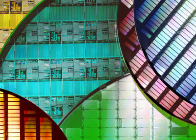
View From a Manufacturer’s Window. Silicon Slice: A Wafer, Cut From an Ingot, Will Be Used in Electronics. From It, We Create Integrated Circuits.
Silicon wafers are the heart of modern technology because, without them, you could not have semiconductors. And semiconductors are in all your favorite devices, like cell phones.
Thus, we thought you might like to know how ER Precision Optics creates silicon crystals to many precise specifications. They are destined to become semiconductors. Let’s look at the steps Silicon goes through to qualify for life as a semiconductor.
The Chicken or the Egg? In the Beginning, Creating the Ingot
We will use the CZ method, as explained in the previous blog. Unlike the old chicken or egg dilemma, we must begin by creating the ingot in order to make the wafers.
As you read, you are going to find the following familiar if you have read the previous blog:
Our furnace will begin the process of cooking up the ingot by heating silicon to 1420 degrees Centigrade. Why do we turn up the heat? It is because that number is above the melting point of silicon.
Relationship Between Ingots and Wafers
Note also the silicon will first become cylindrical ingots and then it will be sliced into wafers. Finally, it will be diced into the familiar-looking size needed for a semiconductor.
However, to create the ingot from polycrystal silicon, we will need a “seed” crystal of the same orientation as the single crystal we wish to grow. This makes the comparison of the chicken and the egg a little more intriguing. You see, the resulting silicon ingot will be identically the same orientation as our initial seed crystal.
A Recipe of Dopants to Create Ingots for Specific Materials
Semiconductors Without Silicon Wafers? Then, Electronic Devices Would Not Work Very Well.
We do not want impurities in our silicon so we will add dopants to the recipe and let them dissolve into the “melt.”
- Usually, we load (or charge) our Semiconductor grade polysilicon into the crucible, in our first step.
- We add carefully measured amounts of dopants like Phosphorus or Boron.
- Likewise, we want to avoid oxidation while we grow the crystal. Thus, “Evacuation removes any air from the chamber…”
- Then, electrically heat the charged crucible to a temperature sufficient to melt the polysilicon (greater than 1421ºC).”
In Remembrance of Czowalski’s Pen Nib: A rod and a Seed Crystal
Do you remember our story of how Czochralski accidentally dipping his pen tip in melted tin? The concept hasn’t changed. Within the chambers of our large furnaces, if you could see with x-ray eyes, you would see a long rod. It is suspended over the melted silicon and dopant mixture. This is exactly how Czochralski’s hand suspended the pen nib over the vat of melted tin.
- At the tip of the rod, in vertical suspension, sits a tiny crystal. We call it the seed crystal.
- And the mechanism initiates the will of the rod with “pull.” The rod will pull the crystal out of the melt, as it grows. This reminds us of the pen nib that pulled a filament from the melted tin in Czochrlski’s accident and experiments.
- Note that the “seed crystal is typically about 5 mm in diameter and up to 300 mm long. It acts as a “starter” for the growth of the larger silicon crystal from the melt.”
Rotation in the Creation Before Ingots Can Become Wafers
Keep in mind that and the ingot must have the same orientation as the seed crystal, at the end of this process. Thus, using your x-ray eyes again, you would see we are rotating the seed crystal and the molten silicon container in opposite directions.
Making Ingots: X-ray Eyes on a Tightly Controlled Process
That rotation process will give the molten silicon and the seed crystal the same orientation. To put it simply, we control the crystal growth to make ingots and wafers, by controlling three things:
1. Firstly, the heat.
2. Likewise, our critical process of controlling the opposing rotation of the seed crystal on the rod and the molten silicon container.
3. Finally, speed is of the essence, not only of the rotation but the withdrawal of the seed crystal on the rod. Actually, it is “the pull speed “that “determines the final diameter of the large crystal.”
Traveling from Ingot to Wafer: Let’s Finish it!
Experts state, “After removing from the melt, and as it starts to cool, the atoms start to orient themselves to the crystal structure of the seed.”
- Typically, the facets of seed crystals have Miller indices of <100>, <110> or <111>.
- The “Aha Moment” will happen when “The crystal growth from the melt will conform to this initial orientation, giving the final large single crystal a known crystal orientation.”
The Miracle of the Moment
After all the above steps, our crystal is now cylindrically shaped. At present we would call it a “boule” or an “ingot.”
Once it has cooled, we can slice the ingot into circular shapes. It’s not exactly like slicing a tube of great grandmother’s cookie dough into cookies, but it is a similar process. Finally, we will slice it into circular shapes we term “wafers.” In fact, it was born for this.
Terrific Take-aways

Grand Ma Sliced Cookies From a Roll of Cold Dough. However, Slicing Wafers From A Silicon Ingot Is Considerably More Complex.
On the way to becoming semi-conductors, manufacturers like us will cut, polish, lap, grind, shape, and etch these wafers. By the way, “lapping” happens when we utilize a counter-rotating lapping machine. The machine smoothes, polishes, flattens and fixes the marks remaining from the diamond saw.
And after all those steps, ER Precision Optics offers our clients custom grades of single and polycrystal material, created to their specifications. Each wafer is carefully inspected and packed before we ship it.
Please remember that ER Precision Optical brings you optical grade as well as solar grade CZ grown material. We would be remiss if we did not remind you that our optical grade materials are pure to (>99.99999%). Also, our solar grade material is up to (<99.999%).
Our Crystal Pledge, Sealed with Ingots and Wafers
Every day, ER Precision Optical renews our commitment to “uphold some of the industry’s tightest specifications for stress-free and finely annealed crystals.” As you must have gathered, crystal growing is a complex and precise craft. It crosses science, art, and manufacturing.
And it’s not all about Silicon, although this article focuses on that element. Every day, we see more custom materials emerging. And ER Precision Optics supports R&D into the amazing world of custom-grown crystals. We have the equipment and staff who can help your company step into the future.
If these facts about creating crystals for semiconductors have fascinated you, you might enjoy visiting a unique online resource, an online Computer Museum.